|
Getting your Trinity Audio player ready...
|
Author: David Richards | Published on: 19/03/25
Introduction
PCB prototyping is a critical step before mass production. It helps identify design flaws, test circuit functionality, and optimize layouts. However, many beginners and even experienced designers make avoidable mistakes that lead to costly revisions. In this guide, we’ll explore common PCB prototyping errors and how to prevent them.
1. Incorrect Trace Widths and Spacing
✅ Why It Matters:
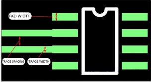
Traces that are too thin can overheat, while traces that are too close can cause short circuits.
🔹 Solution:
- Use an online trace width calculator to determine the correct size based on current requirements.
- Follow the manufacturer’s minimum clearance guidelines (e.g., JLCPCB, PCBWay).
2. Ignoring Design Rule Checks (DRC) & Electrical Rule Checks (ERC)
✅ Why It Matters:
Skipping DRC/ERC in PCB design software can lead to overlapping traces, insufficient clearances, and electrical errors.
🔹 Solution:
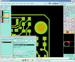
- Always run DRC/ERC checks before exporting Gerber files.
- Configure Eagle, KiCad, or Altium with your manufacturer’s specs.
3. Poor Component Placement
✅ Why It Matters:
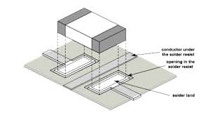
Bad component placement can cause signal integrity issues, inefficient routing, and difficulty in soldering.
🔹 Solution:
- Place high-speed signal components as close as possible to minimize interference.
- Avoid placing components too close to board edges (especially connectors).
4. Forgetting Thermal Relief for Soldering
✅ Why It Matters:
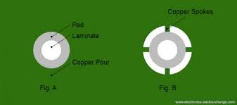
Without proper thermal relief, soldering large copper areas becomes difficult, leading to cold joints.
🔹 Solution:
- Use thermal relief pads around vias and large copper pours.
- Enable the thermal relief option in your PCB design software.
5. Wrong Via Sizes and Annular Rings
✅ Why It Matters:
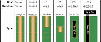
Incorrect via sizes can make it impossible to manufacture your PCB or result in weak connections.
🔹 Solution:
- Check the minimum via sizes required by your PCB manufacturer.
- Use tenting vias for a cleaner design and prevent solder paste from filling holes.
6. Not Generating Gerber Files Correctly
✅ Why It Matters:
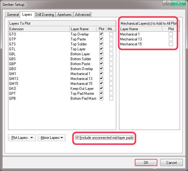
Incorrectly generated Gerber files can lead to missing layers, incorrect drill holes, and failed fabrication.
🔹 Solution:
- Before sending to a manufacturer, view Gerber files using a Gerber Viewer.
- Ensure you include all necessary layers (Top, Bottom, Silkscreen, Drill Files).
Conclusion
PCB prototyping is an essential part of the electronics development process. By following these best practices, you can reduce errors, save time, and avoid costly revisions before sending your design for manufacturing.
🔹 Next Steps:
✅ Double-check your design with DRC/ERC
✅ Use correct trace widths & via sizes
✅ Review your Gerber files before submission
Before committing files to fabrication, use our free PCB footprint pre-order checklist to compare the part drawing, symbol pin numbers, pad geometry and orientation. It includes a connector example and explains what automated checks can miss.
Want a structured review before fabrication? The optional PCB Review Lab toolkit (£9.95) includes a 64-point checklist, worked cases, a workbook and an offline tracker. It is a paid digital download for practising schematic-to-fabrication checks; it does not include a tested PCB design or an individual review service.
If you found this guide helpful, share your PCB prototyping experiences in the comments! 🚀