|
Getting your Trinity Audio player ready...
|
How to Design Your First PCB (Step-by-Step)
Designing your first Printed Circuit Board (PCB) can feel intimidating at first—but once you break it down into clear steps, it becomes an exciting and highly rewarding process. Whether you’re building a simple LED circuit or your first microcontroller project, this guide will walk you through the entire workflow from idea to manufactured board.
- Difficulty: Intermediate
- Time required: N/A
- Tools needed: PC
- 🔧 Components list
- 💰 Estimated cost
- ⚡ Power requirements
- 🧠 Skill level
What Is a PCB?
A Printed Circuit Board (PCB) is a physical board used to connect and support electronic components. Instead of messy wires, PCBs use copper traces etched onto a board to create clean, reliable connections.
Step 1: Define Your Project
Before using any software, decide exactly what you want to build.
Ask yourself:
- What is the purpose of the circuit?
- What components will I need?
- What power source will it use?
Example:
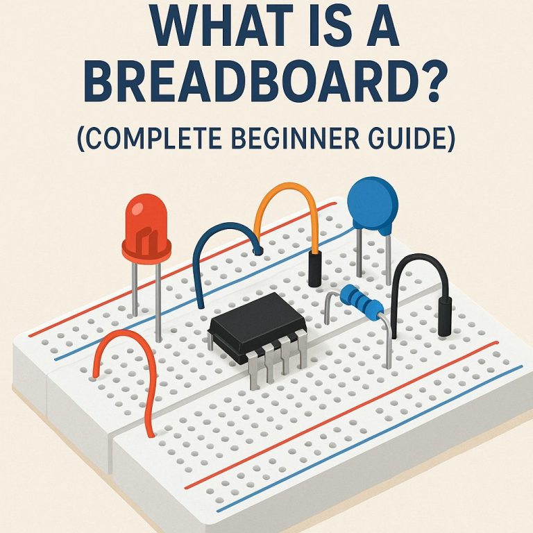
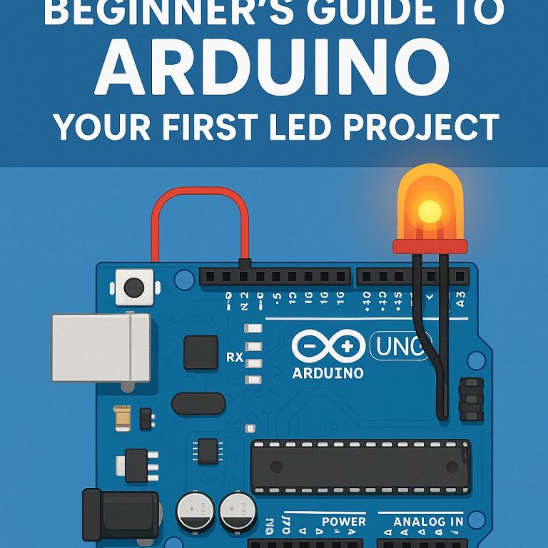
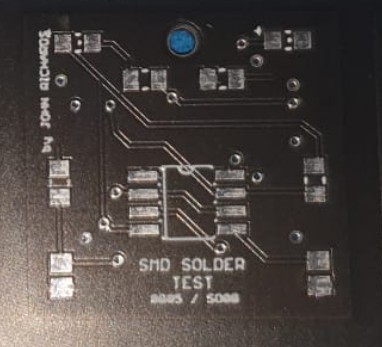
A beginner project could be something like a blinking LED using a timer chip or microcontroller, as shown here.
👉 Tip: Keep your first project simple. Complexity can come later.
Step 2: Create a Circuit Schematic
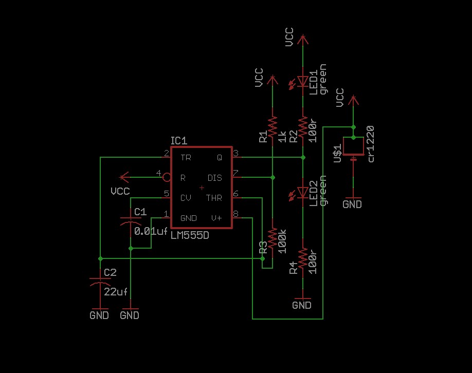
A schematic is a diagram that represents your circuit logically.
You’ll:
- Place components (resistors, LEDs, ICs, etc.)
- Connect them with virtual wires
- Label power (VCC) and ground (GND)
Popular beginner tools:
👉 Focus on correctness here—this is the foundation of your PCB.
Step 3: Choose Your Components
Each component needs a footprint (its physical representation on the board).
Things to consider:
- Through-hole vs Surface Mount (SMD)
- Availability (can you actually buy it?)
- Size (important for layout later)
👉 Beginners often start with through-hole components because they’re easier to solder.
Step 4: Assign Footprints
Now you link each schematic component to a physical footprint.
For example:
- A resistor → axial resistor footprint
- An IC → DIP or SOIC package
👉 Mistakes here can ruin your board, so double-check:
- Pin count
- Pin spacing
- Orientation
Step 5: Create the PCB Layout
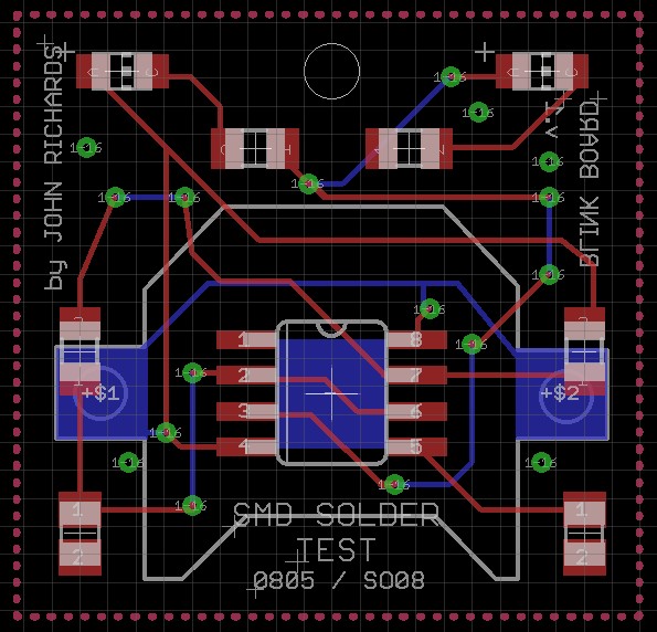
This is where your design becomes physical.
You will:
- Define the board shape
- Place components
- Route copper traces between them
Placement Tips:
- Group related components together
- Keep signal paths short
- Place connectors near edges
Routing Tips:
- Use wider traces for power
- Avoid sharp angles (use 45° bends)
- Keep traces neat and organized
👉 Think of this like solving a puzzle—efficient and clean layouts matter.
Step 6: Add a Ground Plane
A ground plane is a large area of copper connected to ground.
Benefits:
- Reduces electrical noise
- Improves stability
- Simplifies routing
👉 Most PCB tools let you create this automatically with a “fill” or “polygon” tool.
Step 7: Run Design Rule Checks (DRC)
Before manufacturing, your design must pass checks.
These include:
- Minimum trace width
- Clearance between traces
- Proper connections
👉 Always run DRC—this step catches mistakes you might not see.
Step 8: Generate Gerber Files
Gerber files are the standard format used by PCB manufacturers.
They include:
- Copper layers
- Drill holes
- Silkscreen
- Solder mask
👉 Your PCB software will export these for you.
Step 9: Order Your PCB
Upload your Gerber files to a PCB manufacturer like JLCPCB.
Typical options:
- Board size
- Thickness
- Number of layers (start with 2-layer boards)
- Solder mask colour
👉 Many manufacturers offer very cheap prototypes for beginners.
Step 10: Assemble and Test
Once your board arrives:
- Solder components onto the PCB
- Inspect for mistakes (bridges, missing parts)
- Power it up carefully
👉 If it doesn’t work first time—don’t worry. Debugging is part of the learning process.
Common Beginner Mistakes
Avoid these pitfalls:
- Incorrect footprints
- Missing ground connections
- Traces too thin
- Components placed too close together
- Forgetting mounting holes
Pro Tips for Beginners
- Start with simple circuits
- Print your PCB layout on paper to check size
- Label everything clearly on the silkscreen
- Keep a note of what worked and what didn’t
Final Thoughts
Designing your first PCB is a huge milestone. It takes patience, attention to detail, and a willingness to learn from mistakes—but once you hold your own custom board in your hands, it’s incredibly satisfying.