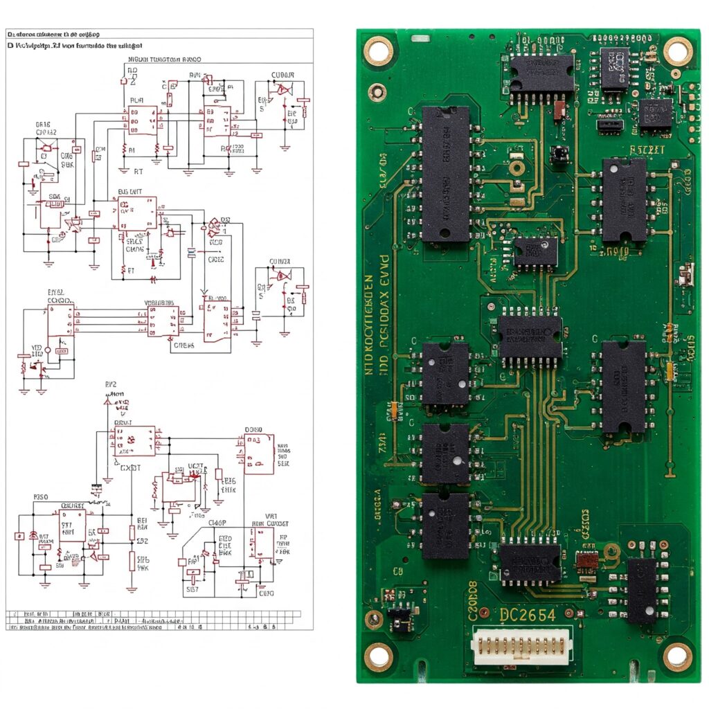
From Schematic to PCB—Bringing Your Electronics Ideas to Life!
I've got a circuit that works on paper. Now how do I turn it into a PCB?
Almost everyone who builds electronics asks this. Perhaps you have a breadboard prototype that behaves only when nobody touches the wires. Perhaps you have a KiCad or EasyEDA schematic and a vague sense that “the next step” involves Gerber files. Or you’re a start-up with a product concept and an engineer who says, “We need a board.”
The jump from schematic to printed circuit board (PCB) is where an idea becomes a manufacturable product. A PCB is far more than a tidy way to connect components. Its layout affects noise, reliability, heat, electromagnetic emissions, assembly yield, mechanical fit and unit cost. A circuit that works on a breadboard can fail on a badly laid-out board, and a good board can make a marginal circuit behave.
This guide follows the whole journey: idea, requirements, schematic, components, layout, manufacture, assembly, test, debug, revision and production. At PCB Electronics we publish beginner-friendly PCB and Arduino projects, tutorials and downloadable Gerber files, so the emphasis here is on understanding the process. Where a decision depends on your board, manufacturer or product, I say so rather than pretending there’s one right answer.
Terminology, once: A PCB (printed circuit board) is a laminate carrying copper tracks that connect components. A PCBA is the populated board, meaning the PCB with components soldered on. Fabrication means making the bare board. Assembly means populating it.