|
Getting your Trinity Audio player ready...
|
From Schematic to PCB—Bringing Your Electronics Ideas to Life!
I've got a circuit that works on paper. Now how do I turn it into a PCB?
Almost everyone who builds electronics asks this. Perhaps you have a breadboard prototype that behaves only when nobody touches the wires. Perhaps you have a KiCad or EasyEDA schematic and a vague sense that “the next step” involves Gerber files. Or you’re a start-up with a product concept and an engineer who says, “We need a board.”
The jump from schematic to printed circuit board (PCB) is where an idea becomes a manufacturable product. A PCB is far more than a tidy way to connect components. Its layout affects noise, reliability, heat, electromagnetic emissions, assembly yield, mechanical fit and unit cost. A circuit that works on a breadboard can fail on a badly laid-out board, and a good board can make a marginal circuit behave.
This guide follows the whole journey: idea, requirements, schematic, components, layout, manufacture, assembly, test, debug, revision and production. At PCB Electronics we publish beginner-friendly PCB and Arduino projects, tutorials and downloadable Gerber files, so the emphasis here is on understanding the process. Where a decision depends on your board, manufacturer or product, I say so rather than pretending there’s one right answer.
Terminology, once: A PCB (printed circuit board) is a laminate carrying copper tracks that connect components. A PCBA is the populated board, meaning the PCB with components soldered on. Fabrication means making the bare board. Assembly means populating it.
1. Start with the electronics idea
Projects that skip requirements tend to pay for it in a second board revision. Before opening any software, write down what the product must do and where it will live.
- Function: what it measures, controls or communicates.
- Inputs and outputs: sensors, buttons, LEDs, displays, relays, motors.
- Power: battery, mains adapter, USB, PoE? Voltage, peak current, battery life?
- Interfaces: UART, SPI, I²C, USB, CAN, Wi-Fi, Bluetooth, Ethernet.
- Processing: microcontroller, single-board computer, FPGA, or no firmware at all.
- Connectors: what plugs in, and from which edge?
- Physical limits: board size, height, enclosure, mounting points.
- Environment: temperature range, moisture, vibration, outdoor use.
- Volume and cost: one board, fifty, or five thousand?
- Safety and regulatory context: mains voltages, radio modules, battery chemistry, target market.
Worked example: a temperature logger idea
“I want a small battery-powered sensor that reports room temperature over Wi-Fi.” Turned into requirements:
| Area | Requirement (illustrative) |
|---|---|
| Function | Measure temperature and humidity; send readings periodically |
| Processing | Wi-Fi-capable microcontroller module |
| Power | Two AA cells or USB-C charging (decision needed) |
| Interfaces | I²C sensor; USB for programming; one status LED |
| Size | Fits a small enclosure; two mounting holes |
| Environment | Indoor, room temperature |
| Volume | 5 prototypes, possibly 200 later |
| Compliance | Contains a radio module, so radio and EMC rules need checking |
That table will drive every later decision, from which regulator you choose to how many layers you need. Our electronics calculators can help with early sums such as resistor values and voltage dividers.
2. Turning the idea into a schematic
A schematic is a symbolic diagram of the circuit. It shows what is connected to what, not where anything physically sits. It uses:
- Symbols for resistors, capacitors, diodes, transistors, ICs, microcontrollers and connectors.
- Nets, the named electrical connections (for example, +3V3, GND, I2C_SDA ).
- Power rails and ground symbols, so you don’t draw every connection as a line.
- Reference designators (R1, C4, U2, J1) that link the schematic, layout and bill of materials.
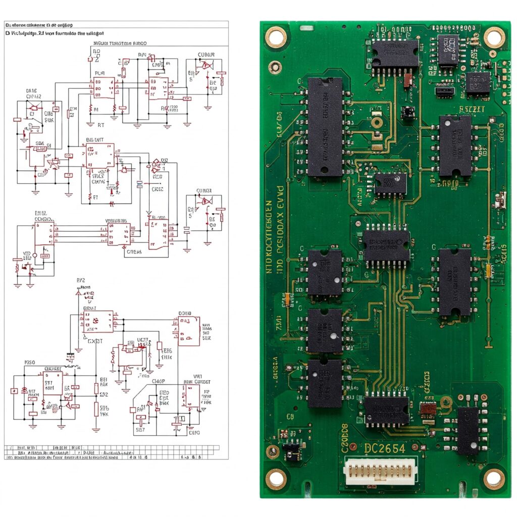
Schematic vs PCB layout
| Schematic | PCB layout | |
|---|---|---|
| Purpose | Defines circuit connectivity and function | Defines the physical board |
| Shows | Symbols, nets, values | Footprints, tracks, planes, vias, outline |
| Main focus | Correct electrical design | Placement, routing, manufacturability, performance |
| Typical mistakes | Wrong pin, missing power, wrong value | Poor placement, thin tracks, bad grounding |
| Used when | Design, review, debugging reference | Fabrication and assembly |
Common schematic mistakes
- Wrong component values, or a resistor divider calculated for the wrong reference voltage (check with the voltage divider worked examples).
- Missing power connections on IC pins that the symbol hides.
- Incorrect pin assignments, such as swapped TX/RX or a function not available on that pin.
- Floating inputs that pick up noise.
- Reversed polarity on electrolytic capacitors, diodes or connectors.
- Missing decoupling capacitors.
- Poorly defined interfaces: no pull-ups on I²C, no ESD protection on exposed connectors.
- A power supply that can’t deliver peak current.
- Wrong footprints attached to correct symbols.
Review the schematic properly before layout. Print it, or have someone else read it, and check every IC against its datasheet pin by pin. Fixing a wire in software costs minutes. Fixing it on manufactured boards costs a respin.
3. Choosing the right components
A component that works electrically may still be a poor choice. Consider:
- Electrical ratings: voltage, current and power, with margin. Check temperature ratings and tolerances too.
- Package: a 0402 passive or a fine-pitch QFN is much harder to hand-solder than a 0805 or SOIC. Package choice decides who can assemble your board and how.
- Availability and lead times: a part you can’t buy is a broken design. Check stock from more than one distributor.
- Lifecycle: look for “not recommended for new designs” or end-of-life notices.
- Cost: at 5 units nobody cares, at 5,000 everybody does.
- Alternatives: where possible, choose parts with pin-compatible second sources, and record approved alternates.
Footprints matter
A footprint (or land pattern) is the copper pad arrangement a component is soldered onto. A wrong footprint is one of the most expensive beginner errors because it’s invisible until the parts arrive. Compare the footprint against the manufacturer’s recommended land pattern, and print the layout 1:1 on paper and hold the real component against it. We cover this in How to Check a PCB Footprint Before Ordering Boards.
For general SMD land-pattern conventions, the IPC-7351 standard (“Generic Requirements for Surface Mount Design and Land Pattern Standard”) is a widely used reference, though many designers rely on libraries and manufacturer recommendations.
4. From schematic to PCB layout
In your EDA (electronic design automation) tool, the process usually runs:
- Assign footprints to every schematic symbol.
- Import the netlist into the PCB editor. This carries components and connections across.
- Define the board outline, plus mounting holes and keep-out areas.
- Set design rules: minimum track width, clearance, via and hole sizes, based on your fabricator’s capabilities.
- Place components.
- Route the tracks and define planes (large copper areas, typically ground or power).
- Add vias (plated holes joining layers).
- Run DRC (design rule check).
- Generate manufacturing files.
Free and low-cost tools include KiCad, EasyEDA and Autodesk Eagle. For a complete beginner walkthrough, see How to Design Your First PCB.
Layout is not drawing. Physical arrangement influences signal integrity, noise, EMI/EMC (emissions and immunity), heat, power delivery, manufacturability, serviceability and mechanical fit, all at once.
5. Component placement: more important than it looks
Placement is an engineering decision, not a tidiness exercise. Good placement makes routing easy. Bad placement makes good routing impossible.
Practical principles
- Group related circuits and keep connected parts close.
- Put decoupling capacitors right at IC power pins, with the shortest practical loop to ground.
- Keep sensitive signal paths short, and keep noisy circuits away from them.
- Place connectors first, because the enclosure decides where cables exit.
- Note heat sources and give them copper area and airflow.
- Leave assembly access: clearance for pick-and-place nozzles, soldering tools, test probes and programming headers.
- Add mounting holes and check clearance against screw heads and standoffs.
- Check the enclosure early, including component height.
Examples
- Microcontroller: crystal close to the oscillator pins, decoupling at each supply pin, reset and programming header reachable.
- Switching regulator: keep the high-current switching loop (input capacitor, switch, inductor, output capacitor) compact, and keep it away from analogue sections.
- Analogue circuits: keep the sensor front-end away from switching noise and digital clocks, with a clean reference.
- High-current parts: put them near the power input, with short, wide copper paths.
- Connectors: place them on the edges they’ll actually be used from, with strain relief in mind.
6. PCB routing and track design
“Just connect everything with tracks” doesn’t produce a professional board. Routing decisions include:
- Track width: depends on current, acceptable temperature rise and voltage drop.
- Track spacing: depends on voltage and on what your fabricator can reliably manufacture.
- Copper thickness: standard and heavy copper have different current capacity and different minimum feature sizes.
- Vias: each adds inductance and resistance, and vias carrying current need sensible sizing.
- Planes: continuous ground and power planes simplify routing and help with noise.
- Special signals: differential pairs, high-speed signals and sensitive analogue lines each need controlled treatment.
IPC-2221 (“Generic Standard on Printed Board Design”) is the long-standing source of conductor-current guidance, and many online calculators derive from it. Treat any calculator as a starting point, and remember that internal and external layers behave differently. No single track width is “correct”.
Why return paths matter
Current flows in loops. Every signal needs a return path back to its source, and at higher frequencies that return current tends to follow the route directly beneath the signal trace on the adjacent plane, because that minimises loop area. If you split or cut the plane under a fast signal, the return current must detour, which creates a larger loop that radiates and picks up noise.
Poor routing can cause noise, crosstalk (signals coupling between neighbouring tracks), voltage drop, EMI problems, signal-integrity failures, heating and intermittent behaviour, the last of which is the hardest to debug.
7. Designing for power and heat
Power and thermal design deserve their own review pass.
- Linear regulators are simple and quiet but dissipate the voltage difference times the current as heat. Always calculate the dissipation.
- Switching regulators are more efficient but generate switching noise and demand careful layout, as the manufacturer’s datasheet and layout guidelines will describe.
- High-current paths: use short, wide copper or pours, and check the voltage drop across them.
- Copper as a heatsink: PCB copper spreads heat. Many power packages rely on an exposed pad soldered to a copper area.
- Thermal vias beneath such pads move heat to other layers. Whether they can be open or must be filled or tented affects assembly, so check with your assembler.
- Heatsinks may be needed for higher dissipation and affect mechanical layout.
- Temperature ratings: check component ratings against ambient plus self-heating, particularly electrolytic capacitors and batteries.
Design rule of thumb: work out the power dissipation of every significant component before layout, and reserve space for the answer.
8. PCB layer stack-up
- Single-layer: copper on one side. Cheap and simple, and only practical for simple circuits.
- Double-sided (2-layer): copper on both sides, joined by plated holes. Very common for hobby and simple products.
- Multilayer (4, 6, 8+): inner layers, typically dedicated ground and power planes plus signal layers.
| Factor | Fewer layers | More layers |
|---|---|---|
| Cost | Lower | Higher |
| Board size | Often larger | Can be smaller |
| Routing density | Limited | Higher |
| Signal integrity / EMI | Needs care in layout | Solid reference planes make it easier |
| Manufacturing complexity | Simpler | More process steps |
Neither is “best”. A simple sensor board may do very well on two layers with a well-planned ground pour. A board with fast interfaces, dense BGAs or demanding EMC requirements often benefits from four or more. Discuss stack-up with your fabricator, because available materials, thicknesses and impedance-control options vary.
9. Design for manufacture (DFM)
Design for Manufacture means designing so the board can be made reliably and economically. A board can pass every electrical check and still be costly or unmanufacturable. Key checks:
- Minimum track width and spacing
- Drill sizes and annular rings (copper ring left around a drilled hole)
- Copper-to-edge clearances
- Solder mask openings and slivers between pads
- Silkscreen legibility and keeping it off pads
- Component spacing for assembly and inspection
- Panelisation: how boards are arrayed on a production panel, including rails, tabs or V-scoring
- Manufacturing tolerances on hole position, outline and layer registration
Different fabricators have different capabilities, so read your chosen manufacturer’s published design rules before routing, not after. Good DFM reduces delays, rework and cost.
General good practice ≠ manufacturer-specific requirement ≠ industry standard. Keep those three straight when someone says a rule is “required”.
10. Design for assembly (DFA)
Design for Assembly looks at how the populated board will be built.
- SMT (surface-mount technology): components sit on pads. Solder paste is applied through a stencil, a pick-and-place machine positions parts, and the board passes through a reflow oven.
- Through-hole: leads pass through holes and are soldered by hand, by wave soldering or by selective soldering.
- Mixed technology boards combine both, which affects process order and cost.
Layout considerations include component orientation (consistent orientation helps assembly and inspection), spacing around tall parts, fiducials (small copper marks used by machine vision for alignment), pad shapes, and access for hand rework.
A board designed for hand assembly, with generous spacing and mixed packages, may need changes before it suits automated production. The reverse is also true: boards packed for automation can be miserable to hand-assemble.
11. Prototype PCB manufacturing
When the design is ready for a first build, you’ll generate:
- Gerber files, one per copper, mask, silkscreen and outline layer
- Drill files
- BOM (bill of materials)
- Pick-and-place (centroid) file giving X, Y and rotation for every part
- Assembly and fabrication drawings
- A board specification: layers, thickness, copper weight, finish, mask colour
Some manufacturers accept alternative formats such as ODB++ or IPC-2581. Ask what yours prefers.
Prototypes are not “small production runs”. Their purpose is learning: does the circuit work, does the board fit, is it easy to assemble and test? Keep revision control from day one, meaning every board carries a revision number on the silkscreen.
When the prototypes arrive: inspect before powering. Check the board against your files, confirm dimensions, check hole and footprint fit with real components, and look for anything the DRC couldn’t tell you.
12. PCB assembly
Bare-board fabrication and assembly are related but distinct stages, and often use different suppliers or different departments.
For an SMT board, the typical flow is:
- Solder paste printing through a stencil.
- Component placement by pick-and-place machine (or by hand for small runs).
- Reflow soldering. In a reflow oven, the board is heated through preheat, soak, reflow and cooling stages so the paste melts and forms joints. The surface tension of molten solder can help align components on correctly designed pads. Wikipedia
- Through-hole assembly where needed.
- Inspection, then cleaning where the process or application requires it.
- Testing.
13. Inspection and testing
A manufactured board isn’t necessarily a working product.
- Visual inspection: bridges, missing parts, tombstoned passives, wrong orientation.
- AOI (automated optical inspection): cameras compare the board with a reference to detect placement and solder defects.
- X-ray inspection: reveals joints you can’t see, such as under BGAs.
- Continuity/electrical testing on bare boards and assemblies.
- In-circuit test (ICT) and flying-probe test check individual components and nets.
- Power-up testing: current-limited first power, rail checks.
- Firmware loading and functional testing.
There are two different questions here. Was the board assembled correctly? Is answered by inspection and structural test. Does the product do its job? Is answered by functional test against your requirements. You need both.
14. Debugging the first PCB
If the first board doesn’t work, resist random part-swapping. Work systematically:
- Check the revision. Are you holding the board you think you are?
- Inspect closely with magnification: bridges, opens, tombstones.
- Check polarity and orientation of diodes, ICs, electrolytics and connectors.
- Power up with a current limit, then check current consumption against expectations.
- Verify every power rail with a multimeter.
- Check clocks and resets with an oscilloscope.
- Test communication interfaces one at a time.
- Compare measurements with expected values from the schematic and datasheets.
- Check firmware separately from hardware.
- Compare the physical board against the schematic, net by net, when nothing else explains the fault.
Write down each finding. A debugging log becomes the change list for revision B.
15. PCB revisions and design iteration
Professional development is iterative: prototype → test → identify problems → modify → manufacture revision → retest. Track:
- PCB revision (on the board itself)
- Schematic revision
- BOM revision, with approved alternates
- Firmware version
- Exact manufacturing files sent
- Test results and change notes
Records matter more the closer you get to production. When a customer reports a fault, you need to know which board, BOM and firmware they have.
16. From prototype to production
Working once is not the same as working every time. Production adds:
| Prototype | Production | |
|---|---|---|
| Quantity | A handful | Tens to thousands |
| Design priorities | Learn, iterate, debug | Yield, repeatability, cost |
| Cost focus | Speed | Unit cost, panel utilisation, test time |
| Testing | Manual, exploratory | Defined test procedures or fixtures |
| Documentation | Informal | Controlled BOM, drawings, work instructions |
| Sourcing | Whatever’s in stock | Supply-chain resilience, approved alternates |
Also consider yield (proportion of boards passing first time), traceability (batch and date codes), quality control, test fixtures, and whether the design needs changes to suit the assembly line. A board that works as a one-off can still need engineering changes before volume production.
17. Compliance, reliability and product requirements
Consider compliance from the start, not at the end. Depending on the product, relevant areas may include:
- EMC (electromagnetic compatibility)
- Electrical safety, particularly with mains or high energy
- RoHS (restricted hazardous substances)
- UKCA and CE marking
- Radio equipment rules, if you use Wi-Fi, Bluetooth or other radio modules
- Environmental and reliability requirements: temperature, vibration, moisture, ingress protection
- Product-specific standards
GOV.UK guidance says Great Britain continues to recognise CE marking alongside or in place of UKCA for many product regulations, under the Product Safety and Metrology (Amendment) Regulations 2024. Requirements differ by product category and market, and Northern Ireland has its own arrangements. GOV.UK
Important: this is general information, not legal advice. Which requirements apply depends on your product, intended use, market and jurisdiction. Not every product needs every certification. Take professional compliance advice for a commercial product.
18. Common PCB design mistakes
| Mistake | Why it matters | How to avoid it |
|---|---|---|
| Designing without knowing the manufacturing process | Boards that can’t be made or assembled | Read fabricator and assembler rules first |
| Incorrect footprints | Parts won’t fit | Verify against datasheets; print 1:1 |
| Poor component placement | Noise, routing dead ends | Place with function in mind |
| Inadequate decoupling | Resets, instability | Capacitors at every IC supply pin |
| Insufficient track width | Heating, voltage drop | Calculate current; use calculators as a guide |
| Poor grounding | Noise, unreliable readings | Continuous ground reference where possible |
| Ignoring return paths | EMI, crosstalk | Don’t cut planes under fast signals |
| Forgetting mounting holes | Board can’t be fixed | Include in requirements |
| Ignoring enclosure dimensions | Board doesn’t fit | Import the mechanical outline early |
| No DFM review | Delays, extra cost | Review before ordering |
| Poor documentation | Can’t rebuild or support | Keep controlled files |
| No test strategy | Slow, uncertain debugging | Add test points and programming headers |
| Ignoring component availability | Board can’t be built | Check stock and lifecycle |
| Weak revision control | Confusion about what’s in the field | Version everything |
19. What files are needed to manufacture a PCB?
| File/document | Purpose |
|---|---|
| Gerber files | PCB fabrication data: copper, mask, silkscreen, outline |
| Drill files | Hole positions and sizes |
| Bill of Materials (BOM) | Every component, quantity, reference and part number |
| Pick-and-place file | Component X/Y/rotation for automated placement |
| Assembly drawing | Reference for assembly and inspection |
| Schematic | Circuit reference for assembly, test and debugging |
| PCB layout | Physical board source data |
| Fabrication drawing/notes | Layers, materials, thickness, finish, tolerances |
| Test documentation | Production test procedure and acceptance criteria |
Exact requirements vary by manufacturer and assembly process, so ask before you send files.
20. Working with a professional PCB partner
Many people make excellent first boards themselves. There are also good reasons to bring in professionals:
- Limited in-house PCB layout expertise
- Tight deadlines
- Complex boards: fine-pitch, BGA, RF or high-speed
- Production quantities that need automated assembly
- Turnkey assembly and component sourcing
- A formal DFM review
- Test fixtures and production test
- Scaling from prototype to production
A specialist fabricator or assembler can also spot problems your EDA tool can’t. When choosing one, ask about their published design rules, DFM review process, inspection and test capabilities, quality standards that they can evidence, and how they handle component substitutions.
Where PCB Electronics fits: we’re a learning resource. You’ll find projects at every level, downloadable Gerber files, calculators and how-to guides to help you reach the point where you know what to ask a professional partner.
A practical example: a compact IoT temperature monitor
This is a fictional walkthrough to illustrate the stages, not a documented PCB Electronics project.
- Idea: a battery-powered Wi-Fi sensor that reports temperature.
- Requirements: as in the table earlier, plus a target run of 5 prototypes.
- Schematic: a Wi-Fi microcontroller module, a temperature and humidity sensor on I²C, a regulator, a USB-C connector, a status LED and a programming header. Review finds the sensor’s I²C pull-ups are missing, so they’re added.
- Component selection: the designer swaps a hard-to-source regulator for a pin-compatible alternative with stock, and chooses 0603 passives so prototypes can be hand-soldered.
- Layout: the module’s antenna sits at the board edge with copper cleared beneath it, following the module datasheet. The sensor is placed away from the regulator and module so self-heating doesn’t skew readings. The regulator and its capacitors form a compact loop.
- DFM: the design is checked against the fabricator’s published minimum track, spacing and drill rules. One silkscreen label overlaps a pad and is moved.
- Prototype: five boards are fabricated and hand-assembled.
- Testing: first power-up with a current limit. The board draws far more than expected in sleep mode.
- Debug: the fault is traced to a floating enable pin. It’s a schematic error, not a soldering fault.
- Revision B: the fix, plus a test-point cluster, a corrected mounting-hole position and a version number on the silkscreen.
- Production: for a run of 200, the designer adds fiducials, panelises the board, freezes the BOM with approved alternates, and writes a short functional test procedure.
The “idea to PCB” checklist
☐ Define requirements: function, power, interfaces, size, environment, volume, compliance
☐ Create schematic: named nets, power, decoupling, protection
☐ Review schematic: pin-by-pin against datasheets, ideally by a second person
☐ Select components: ratings, package, availability, lifecycle, alternates
☐ Verify footprints: against datasheet land patterns; print 1:1
☐ Design PCB layout: outline, mounting holes, keep-outs, design rules from the fabricator
☐ Review placement: decoupling, connectors, heat, enclosure fit, assembly access
☐ Route PCB: track widths, return paths, planes, sensitive signals
☐ Run DRC and fix every warning or justify it
☐ Perform a DFM review: check against manufacturer capabilities
☐ Generate manufacturing files: Gerbers, drills, BOM, pick-and-place, drawings
☐ Manufacture prototype: with a revision marking on the board
☐ Assemble PCB: hand or automated, matched to the design
☐ Inspect and test: visual/AOI, power-up, functional
☐ Debug systematically: revision, power, clocks, interfaces, firmware
☐ Revise: fix, version, document
☐ Prepare for production: sourcing, panelisation, test procedure, controlled documentation
Frequently asked questions
What’s the difference between a schematic and a PCB?
A schematic shows how components connect electrically. A PCB is the physical board that implements those connections with copper tracks, footprints and holes.
How do I turn a schematic into a PCB?
Assign footprints, import the netlist to the layout editor, define the outline and design rules, place components, route, run DRC and export manufacturing files.
What software is used for PCB design?
Common options include KiCad, EasyEDA, Autodesk Eagle and Altium Designer. Beginners often start with KiCad or EasyEDA.
How much does PCB design cost?
It varies enormously with complexity, layer count, whether you design in-house or outsource, and testing needs. Get quotes against a clear specification. I haven’t quoted numbers because any figure would be misleading without a specific design.
How long does PCB manufacturing take?
Lead times depend on the manufacturer, board specification, quantity and shipping. Check current lead times with your chosen supplier.
What files are needed to manufacture a PCB?
Typically, Gerber and drill files for the bare board. For assembly, add a BOM and a pick-and-place file, and often assembly drawings. Requirements vary by manufacturer.
What is PCB assembly?
PCB assembly (PCBA) is populating a bare board with components and soldering them, followed by inspection and test.
What’s the difference between SMT and through-hole assembly?
SMT parts sit on surface pads and are usually placed by machine and reflow-soldered. Through-hole parts have leads inserted through holes and are soldered by hand, wave or selective soldering. Many boards use both.
How many PCB layers do I need?
It depends on routing density, signal speeds, EMC goals and cost. Simple circuits often work on two layers. Denser or faster designs often benefit from four or more.
What is DFM?
Design for Manufacture: adapting the design to your manufacturer’s capabilities so boards can be made reliably and economically.
How do I prepare a PCB for mass production?
Freeze and control the BOM, check component supply, add fiducials, consider panelisation, define a production test, document everything, and run a pilot batch before committing to volume.
Can a PCB manufacturer also assemble the board?
Some do, some don’t. Fabrication and assembly are separate processes, and some suppliers offer both as a turnkey service. Confirm with each supplier.
Why should I prototype a PCB?
To find design, fit and assembly problems cheaply before committing to production.
What happens if my first PCB doesn’t work?
That’s normal. Debug systematically (power, clocks, interfaces, firmware, then a physical comparison against the schematic), record findings, and fix them in the next revision.
When should I use a professional PCB design service?
When the design is complex (RF, high-speed, dense), the schedule is tight, or the product is heading for production and compliance.
Ready for the next step?
Whether you’ve just drawn your first schematic or you’re holding a prototype that almost works, the next step is usually a review: of requirements, footprints, placement and manufacturability. Start with our step-by-step first-PCB guide, browse projects by skill level, or try the calculators.
Got a question about your own design? Get in touch through our contact page and tell us what you’re building.