
|
Getting your Trinity Audio player ready...
|
An EEPROM programmer is useful whenever a project needs data that survives a power cycle: calibration values, device settings, lookup tables or a small configuration image. This build uses an Arduino Uno Rev3 to read and write a removable 24LC256 serial EEPROM. You will wire the circuit on a breadboard, upload a sketch that accepts commands through the Serial Monitor, then write, read back and verify individual bytes.
The project is scoped to the 24LC256 and electrically compatible parts with the same memory organisation. EEPROMs are not interchangeable simply because their names look similar: a parallel AT28C256 needs a different programmer, although it also has 256 Kbits of storage. This tutorial gives you a complete bench setup and explains the limits you should check before changing the device.
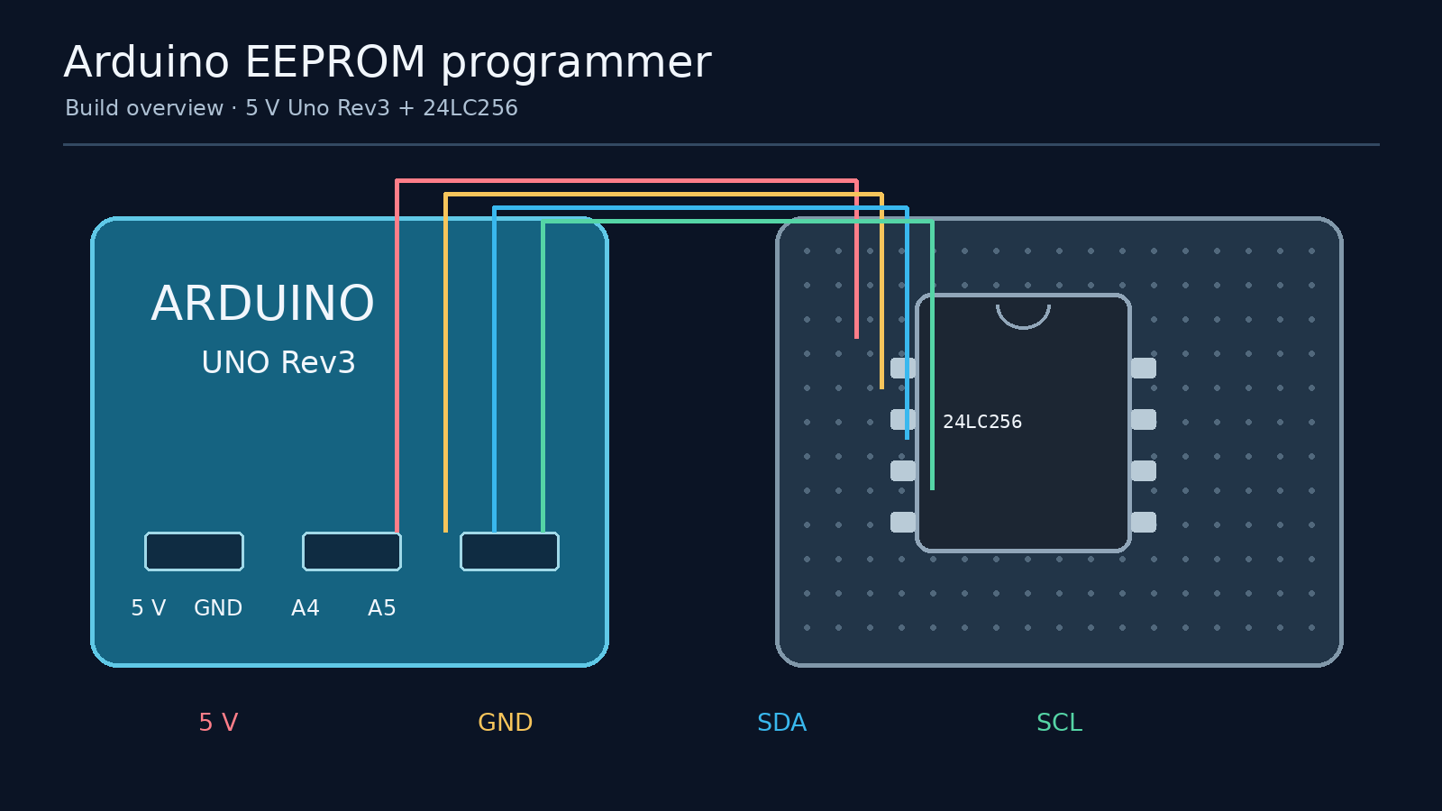
How This EEPROM Programmer Works
EEPROM stands for electrically erasable programmable read-only memory. Unlike the Uno’s working RAM, it retains data after power is removed. Microchip’s 24LC256 stores 256 Kbits, organised as 32,768 eight-bit bytes. Its byte addresses run from 0x0000 through 0x7FFF. The 24LC256 operates from 2.5 V to 5.5 V, allowing it to share a 5 V supply and logic levels with a genuine Uno Rev3. Check the marking and exact device datasheet when substituting a chip.
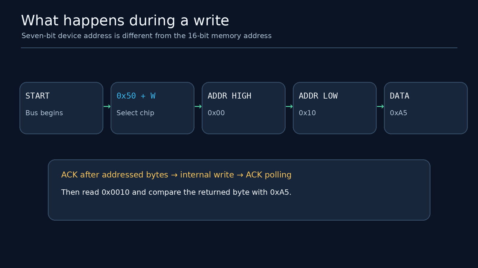
The Uno communicates over I²C, a two-wire bus. SCL carries the clock and SDA carries data. Both lines require pull-up resistors because devices pull the lines low and release them to represent high. Three hardware address inputs, A0–A2, select the chip’s I²C address. Grounding all three selects the seven-bit address 0x50. This is the address of the chip on the bus; a separate two-byte memory address selects a byte inside it.
To write, the Uno sends the chip address, high and low memory-address bytes, then a data byte. The EEPROM starts an internal write cycle and temporarily stops acknowledging commands. The sketch polls for an acknowledgement before reading the address back for verification. For a read, the Uno selects a memory location, then requests one byte. The 24LC256 supports 64-byte page writes, but this first version writes one byte per command to make each transaction easy to inspect and to avoid page-wrap mistakes.
The chip’s WP input controls write protection. Ground it for this programmer; a high level protects the memory array. A successful I²C acknowledgement proves the chip responded, while a read-back comparison checks the data that was actually stored.
Components Required
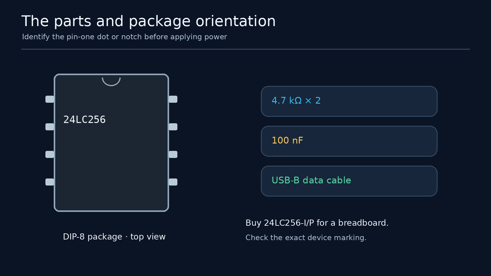
The prices below are indicative UK budgeting allowances, not live quotes. Prices and availability change, and postage may cost more than the small parts. Order the 24LC256-I/P eight-pin through-hole package for a breadboard; a surface-mount version requires an adapter. Choose a data-capable USB cable, rather than a charging-only cable.
| Component | Specification | Approximate cost | Where to source |
|---|---|---|---|
| Microcontroller board | Arduino Uno Rev3, 5 V logic | £20–£30 | Arduino, RS or Farnell |
| EEPROM | Microchip 24LC256-I/P, 32K × 8, DIP-8 | £2–£6 | Mouser, RS or Farnell; verify package and stock |
| Breadboard | Small solderless breadboard | £3–£7 | RS, Farnell or electronics suppliers |
| Pull-up resistors | Two 4.7 kΩ, ¼ W resistors | Under £1 for the pair | RS, Mouser or resistor assortment |
| Decoupling capacitor | 100 nF ceramic | Under £1 | RS, Mouser or component assortment |
| Jumper wires | Approximately ten breadboard jumpers | £2–£5 | Electronics suppliers |
| USB cable | USB-A to USB-B data cable | £2–£6 | Arduino or electronics suppliers |
| Optional socket | Eight-pin DIP socket for a soldered board | Under £1 | RS, Mouser or Farnell |
The 4.7 kΩ pull-ups are a practical starting choice for a short, 5 V breadboard bus, rather than a universal I²C value. The 100 nF capacitor sits close to the chip and stabilises its local supply. If you already own an Uno, cable and breadboard, this project needs few additional parts.
Circuit Diagram and Schematic Explanation
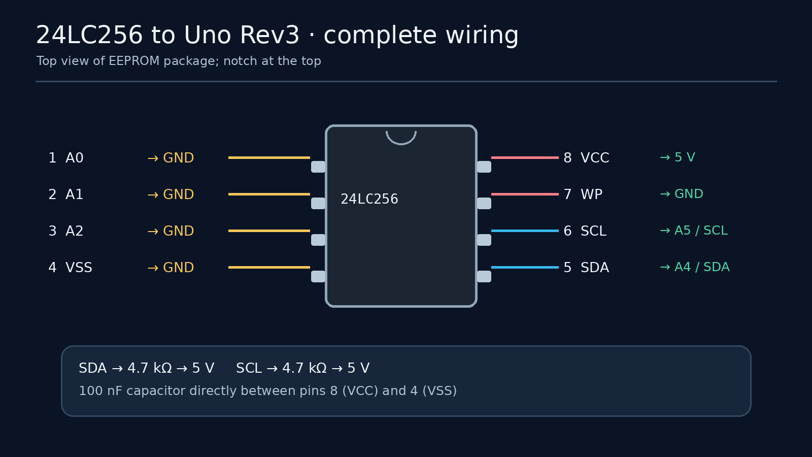
With the DIP package’s notch at the top, pin 1 is at the upper left. Numbering runs down the left side, then up the right side. Confirm the orientation against the package drawing before connecting USB. The Uno Rev3 connects SDA at A4 and SCL at A5; its dedicated SDA and SCL headers expose the same signals. Use one convenient pair of header positions. See the official Uno Rev3 pinout.
| 24LC256 pin | Signal | Connection | Purpose |
|---|---|---|---|
| 1 | A0 | GND | Device address selection |
| 2 | A1 | GND | Device address selection |
| 3 | A2 | GND | Device address selection |
| 4 | VSS | GND | Supply return |
| 5 | SDA | Uno A4; 4.7 kΩ to 5 V | Bidirectional data |
| 6 | SCL | Uno A5; 4.7 kΩ to 5 V | Bus clock |
| 7 | WP | GND | Enable writing |
| 8 | VCC | Uno 5 V | EEPROM supply |
Place the 100 nF capacitor directly across pins 8 and 4, close to the package. One 4.7 kΩ resistor goes from SDA to 5 V; the other goes from SCL to 5 V. Neither belongs in series with a signal. The Uno and EEPROM must share ground. If WP floats or is connected high, reads may work while writes do not. For a later PCB, a clearly labelled two-position write-protect jumper makes this input more useful.
Step-by-Step Build Instructions
1. Identify and place the EEPROM
Disconnect the Uno’s USB cable. Find the chip’s notch or pin-one dot and place it across the breadboard’s centre gap, giving each pin a separate row. Mark the pin-one end on a quick wiring sketch. A photograph of another EEPROM is not a substitute for checking the marking on the component you actually have.
2. Wire power and decoupling
Connect Uno 5 V to EEPROM pin 8 and Uno GND to pin 4. Fit the 100 nF capacitor between those pins as close to the chip as possible. Connect pins 1, 2 and 3 to ground individually to select device address 0x50. Connect pin 7, WP, to ground to permit writes. Some breadboards split their power rails halfway along, so check that every rail segment you use really has its intended connection.
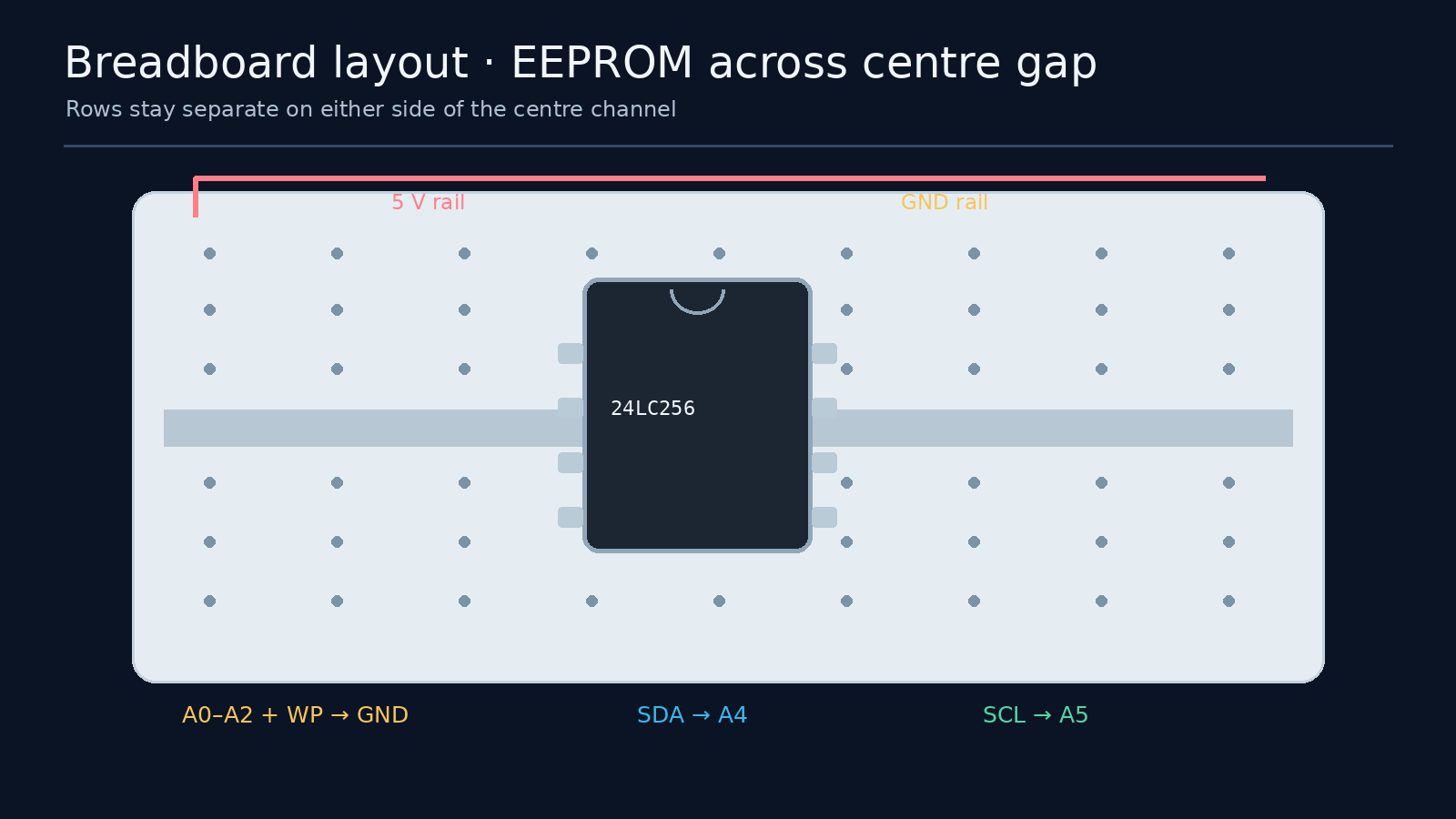
3. Connect the two bus lines
Join pin 5 to Uno A4/SDA and pin 6 to Uno A5/SCL. Fit a 4.7 kΩ resistor between pin 5’s row and 5 V, and another between pin 6’s row and 5 V. Keep the jumpers short and traceable. SDA and SCL sit side by side on the EEPROM and are easily swapped when viewed from the opposite side of the board.
4. Inspect, then power the circuit
Trace pins 1 through 8 against the wiring table. Check the notch, capacitor placement, pull-ups and any split power rails. With USB disconnected, use a multimeter to check for an unintended short between 5 V and ground if one is available. Then power the Uno through USB. Do not leave the EEPROM connected to a second powered circuit during programming: two controllers could attempt to drive its I²C bus.
5. Upload and open Serial Monitor
Select Arduino Uno and its serial port in the Arduino IDE. Upload the sketch below. Set the Serial Monitor to 115200 baud and Newline. The sketch prints a command reminder at startup. Start with a memory location whose old contents can be overwritten.
Arduino Code and Walkthrough
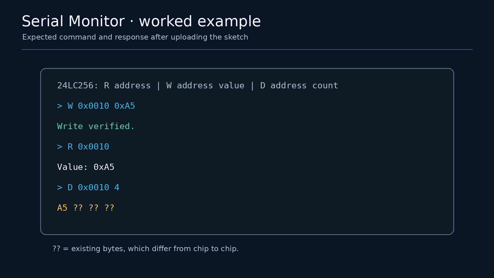
The commands are R address to read one byte, W address value to write and verify one byte, and D address count to show up to 16 consecutive bytes. Numbers can be decimal or prefixed with 0x for hexadecimal. For example, W 0x0010 0xA5 writes 0xA5 to location 0x0010. The complete sketch is:
#include <Wire.h>
#include <stdlib.h>
#include <string.h>

const uint8_t EEPROM_I2C = 0x50;
const uint16_t LAST_ADDRESS = 0x7FFF;
char line[48];
uint8_t used = 0;

bool number(const char *text, unsigned long &value) {
  if (text == NULL || *text == '\0' || *text == '-') return false;
  char *end;
  value = strtoul(text, &end, 0);
  return end != text && *end == '\0';
}

bool selectAddress(uint16_t address) {
  Wire.beginTransmission(EEPROM_I2C);
  Wire.write((uint8_t)(address >> 8));
  Wire.write((uint8_t)(address & 0xFF));
  return Wire.endTransmission(false) == 0;
}

bool readByte(uint16_t address, uint8_t &value) {
  if (!selectAddress(address)) return false;
  if (Wire.requestFrom(EEPROM_I2C, (uint8_t)1) != 1) return false;
  value = Wire.read();
  return true;
}

bool writeByte(uint16_t address, uint8_t value) {
  Wire.beginTransmission(EEPROM_I2C);
  Wire.write((uint8_t)(address >> 8));
  Wire.write((uint8_t)(address & 0xFF));
  Wire.write(value);
  if (Wire.endTransmission() != 0) return false;

  unsigned long start = millis();
  do {
    Wire.beginTransmission(EEPROM_I2C);
    if (Wire.endTransmission() == 0) return true;
  } while (millis() - start < 20);
  return false;
}

void printHex(uint8_t value) {
  if (value < 0x10) Serial.print('0');
  Serial.print(value, HEX);
}

void handleLine(char *input) {
  char *command = strtok(input, " \t");
  char *addressText = strtok(NULL, " \t");
  char *argumentText = strtok(NULL, " \t");
  char *extra = strtok(NULL, " \t");
  unsigned long address, argument;
  if (command == NULL) return;
  if (extra != NULL || !number(addressText, address) ||
      address > LAST_ADDRESS) {
    Serial.println(F("Use R address, W address value, or D address count."));
    return;
  }

  if (strcmp(command, "R") == 0) {
    if (argumentText != NULL) {
      Serial.println(F("R takes one address."));
      return;
    }
    uint8_t value;
    if (!readByte((uint16_t)address, value)) {
      Serial.println(F("Read failed: check the I2C wiring."));
      return;
    }
    Serial.print(F("Value: 0x"));
    printHex(value);
    Serial.println();
    return;
  }

  if (strcmp(command, "W") == 0) {
    if (!number(argumentText, argument) || argument > 0xFF) {
      Serial.println(F("W needs a byte value from 0 to 255."));
      return;
    }
    if (!writeByte((uint16_t)address, (uint8_t)argument)) {
      Serial.println(F("Write failed or timed out."));
      return;
    }
    uint8_t actual;
    if (!readByte((uint16_t)address, actual)) {
      Serial.println(F("Written, but verification read failed."));
      return;
    }
    Serial.println(actual == (uint8_t)argument
                     ? F("Write verified.")
                     : F("Verification mismatch."));
    return;
  }

  if (strcmp(command, "D") == 0) {
    if (!number(argumentText, argument) || argument < 1 ||
        argument > 16 || argument > 32768UL - address) {
      Serial.println(F("D needs 1-16 bytes within EEPROM range."));
      return;
    }
    for (unsigned long i = 0; i < argument; ++i) {
      uint8_t value;
      if (!readByte((uint16_t)(address + i), value)) {
        Serial.println(F("\nDump stopped: read failed."));
        return;
      }
      printHex(value);
      Serial.print(i + 1 == argument ? '\n' : ' ');
    }
    return;
  }
  Serial.println(F("Unknown command: use R, W or D."));
}

void setup() {
  Serial.begin(115200);
  Wire.begin();
  Wire.setClock(100000);
  Serial.println(F("24LC256: R address | W address value | D address count"));
  Serial.println(F("Examples: R 0x0010 | W 0x0010 0xA5 | D 0x0010 4"));
}

void loop() {
  while (Serial.available()) {
    char incoming = Serial.read();
    if (incoming == '\r') continue;
    if (incoming == '\n') {
      line[used] = '\0';
      handleLine(line);
      used = 0;
    } else if (used < sizeof(line) - 1) {
      line[used++] = incoming;
    } else {
      used = 0;
      Serial.println(F("Command too long."));
    }
  }
}
How the code is organised
Wire.begin() starts the Uno’s I²C interface, and Wire.setClock(100000) selects a 100 kHz clock. The constants fix this implementation to seven-bit chip address 0x50 and the 24LC256’s final byte address 0x7FFF. The command parser checks for missing values, bytes over 255, addresses beyond the chip and a dump that would cross the end of memory before issuing transactions.
selectAddress() sends the high memory-address byte, then the low byte. Its endTransmission(false) requests a repeated start for the following read. readByte() demands exactly one returned byte. A missing response becomes an error message, avoiding a plausible-looking value when the bus is disconnected.
writeByte() sends one data byte, then polls for the EEPROM’s acknowledgement while its internal write runs. A 20 ms software timeout prevents endless polling if the wiring is wrong. The W handler immediately reads the same address again and compares the result. That verification tests the stored byte, not merely whether the chip accepted the I²C transaction. The D handler repeats single-byte reads across a short range; it is an inspection command rather than a fast full-chip downloader.
The F() macro holds fixed Serial messages in program memory, preserving the Uno’s limited RAM. The line buffer accepts short commands terminated by Newline and discards an excessively long command rather than attempting to parse incomplete input.
Testing and Calibration
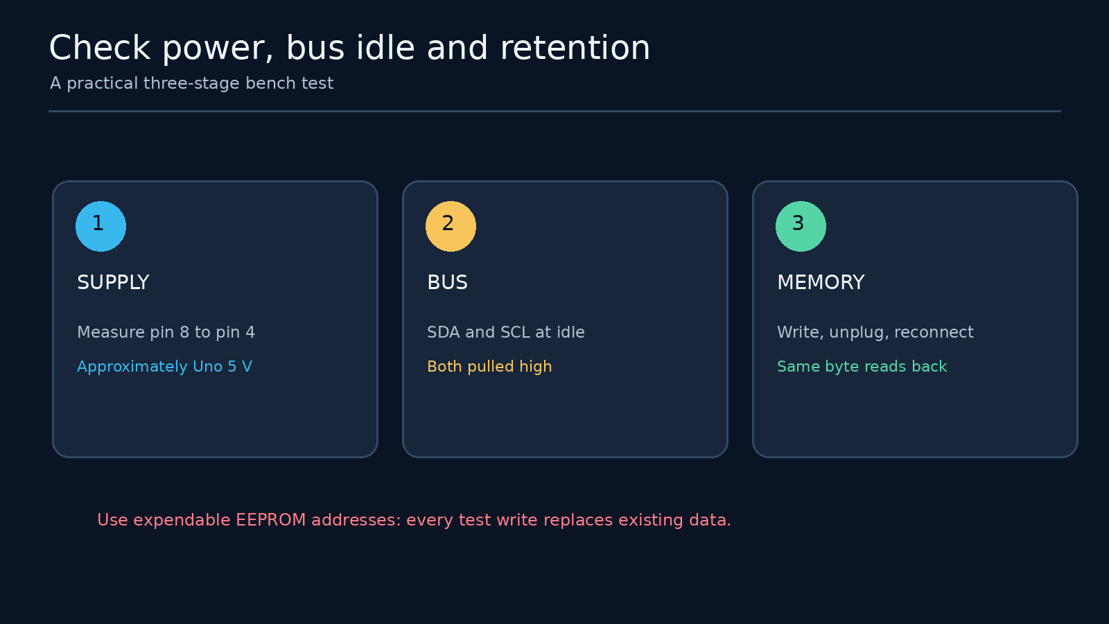
This digital programmer has no analogue calibration control. Testing means checking supply voltage, bus response, address range, write verification and data retention. First measure between EEPROM pins 8 and 4 while powered, if you have a multimeter. It should be close to the Uno’s 5 V rail. An idle SDA and SCL should each read high because of their pull-up resistors. If either stays low, inspect its row and jumper before attempting more commands.
A test write replaces the old byte at that address. Choose an expendable location, then type the following lines separately into Serial Monitor:
W 0x0010 0xA5
R 0x0010
D 0x0010 4
Expect Write verified., then Value: 0xA5. The first byte of the dump should be A5; the other three bytes reflect whatever is already in that particular chip. Never assume an EEPROM arrives filled with FF. Write a second value, such as 0x5A, to the same expendable location and verify it to exercise both zero-to-one and one-to-zero changes in the byte.
Disconnect USB, reconnect and read 0x0010 again. Its last written value should remain after power is removed. Finally, exercise the high end of the address range with an expendable location such as 0x7FFF, and check that R 0x8000 is rejected. These checks cover retention and a boundary that simple low-address tests miss.
For an optional oscilloscope or logic-analyser check, connect the probe ground to circuit ground and inspect SDA and SCL. Both should be high at idle and pulse during a command. An analyser can decode the seven-bit 0x50 chip address and two memory-address bytes. Some analysers instead display address-plus-read/write bytes, so check the display convention before concluding that the address is wrong.
Troubleshooting Common Issues
| Symptom | Likely cause | Practical check |
|---|---|---|
| Every read fails | Wrong chip orientation, missing power, swapped SDA/SCL or wrong address | Check pins 4 and 8; trace pins 5 and 6 to A4 and A5; ground A0–A2 |
| Reads work but writes fail | WP high or disconnected, or unfinished write cycle | Ground pin 7 and retry a single byte |
| Write succeeds but verification mismatches | Poor contact, unstable supply or wrong part | Reseat chip, inspect capacitor and check exact component marking |
| SDA or SCL stays low at idle | Short, misplaced jumper or another bus device | Power off and inspect that line and its pull-up |
| Nothing appears in Serial Monitor | Wrong port, baud rate or line ending | Select uploaded Uno port, 115200 baud and Newline |
| Several bytes look unexpected | Address or value interpreted in wrong number base | Prefix hex numbers with 0x; bare command numbers are decimal |
If another module shares this bus, account for its existing pull-up resistors: several parallel pull-up pairs reduce the effective resistance. For this standalone breadboard, install just the two specified resistors. If problems persist, check the exact EEPROM datasheet. Different capacity, voltage range, package or address scheme can produce confusing results even when another eight-pin chip fits the socket.
Possible Upgrades and Variations
Write-protect switch
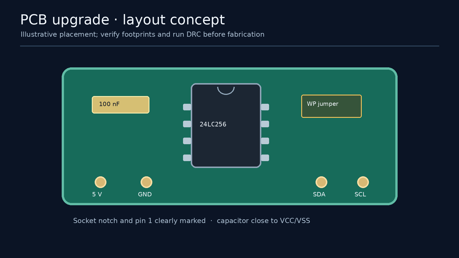
Add a labelled jumper or switch that deliberately connects WP to ground for writing or to 5 V for protection. This is useful when you often read a configuration chip but want to avoid accidental edits. Mark the safe state on the finished board.
Page writes and image transfers
A more capable version could accept a file over USB serial, divide the data at the 24LC256’s 64-byte page boundaries, write each page, poll for completion and compare the resulting bytes. Avoid a transaction that crosses a page boundary: it can wrap within the page rather than continue as a simple linear write. Check both the chip datasheet and your Arduino core’s Wire buffer size when choosing transfer chunks. Include a checksum or full-image comparison in a production workflow.
Dedicated programmer PCB
After the breadboard passes repeated power-cycle tests, move the circuit onto a PCB with an eight-pin socket, a prominent pin-one marker, labelled SDA/SCL test points and the capacitor close to the socket. A socket lets you replace chips without reheating solder joints. Consider a write-protect jumper and enough room around the socket to remove the chip cleanly.
Multiple devices or another controller
A0–A2 allow separate compatible EEPROMs on the same bus if each uses a distinct chip address; this selects another device, not another bank inside one chip. A 3.3 V controller needs a fresh check of supply and pull-up voltages for every bus participant. The EEPROM’s supported supply range alone does not establish that an arbitrary controller board is electrically compatible.
Where an EEPROM Programmer Is Useful
A removable serial EEPROM lets you prepare data away from the circuit that will ultimately use it. Examples include an instrument’s calibration or lookup table, known initial settings for a controller, and a repeatable memory image for teaching I²C addressing. Reading a chip back can reveal how a prototype’s settings changed during testing.
The build also makes communication observable. You can check its supply, inspect bus activity, write a chosen byte and verify persistence. Record valuable existing contents before issuing W commands. The simple sketch is a learning and bench tool; larger transfers call for file import, page handling, full verification and a dependable copy of the source data.
Conclusion
This EEPROM programmer turns an Uno Rev3, a 24LC256 and a handful of passive parts into a practical read-and-write bench tool. Its defined pin map, address checks, acknowledgement polling and immediate verification give you a sound starting point. Write one expendable byte, prove it survives a power cycle, and expand the transfer functions when your application calls for them.
For a complementary site project, see our Arduino EEPROM Programmer PCB introduction. To turn this breadboard version into a durable board, start with our first-PCB design guide, or contact PCB Electronics about a PCB design.
References and further reading
Microchip 24AA256/24LC256/24FC256 datasheet covers the device pinout, operating limits, addressing and write cycles. The Arduino Uno Rev3 pinout identifies SDA, SCL and power headers. The Arduino language reference covers the Wire and Serial APIs.
